CT Inspection of Additive Manufactured Components
Computed Tomography for Additive Manufacturing
Rapidly expanding into production manufacturing, additive manufacturing (AM) has gained incredible interest in all industry facets. From aerospace applications to simple one off consumer home builds, this technology has immense versatility and use. In additive manufacturing, objects are built by adding layer upon layer of material.
With all of these materials in use and knowing that many of these components will be created for critical end use applications in aerospace, medical, or automotive industries to name a few. The challenge becomes; how does the manufacturer inspect these products to ensure safety and longevity as seen with the previous manufacturing methods.
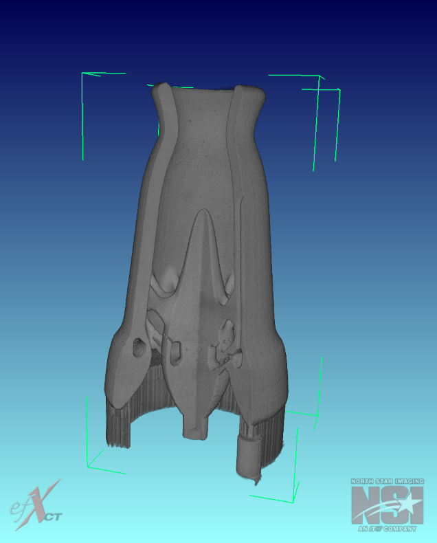
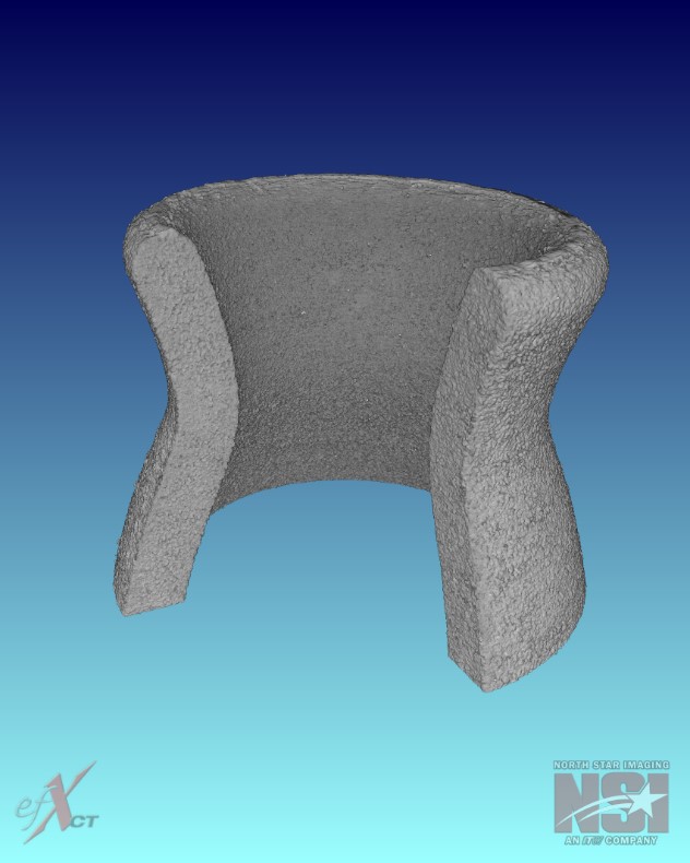
Computed Tomography is a unique and powerful tool, in that we will be able to inspect the component for defects or anomalies, take internal and external metrology measurements, and create a model or drawing from the component. A key benefit of this technology is, this is a Non-Destructive inspection method / technique, and we are not destroying the component in order to extract our data. This allows for inspection of components and the ability to use the end product as intended.
The basic principles of Computed Tomography (CT) are, we image the component and gather a specific number or 2D radiographs, typically done in 360 degrees of rotation. These radiographs are then processed through software which will generate a CT volume of the data. This data is now displayed as 3 dimensional voxel data, producing a 3D image which can be manipulated. The manipulation will include rotation, flip, specific angles, and clip planes which allow the operator to now cut through the sample in multiple directions for evaluation. From the volume clip plane a 2 dimensional image can be generated allowing the user to further enhance the area of interest, and also take measurements at this point.
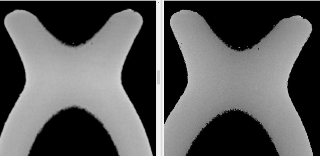
For this discussion, a component made of Titanium was created and imaged at two different voxel resolutions in order to show the capability of locating indications of which may be concerning. A key term to understand will be resolution, referring to the single voxel size of data captured from the imaging devices (digital detector array) 2 dimensional pixel. The more magnification that can be applied to the area of interest or object, the smaller or better the resolution will become. So a 10 micron scan will resolve and display indications much better than a 50 micron scan. The one hurdle here is, depending on part size or area of interest, you may only be able to achieve a certain scan resolution on a specific size of part. Physical limitations will be; moving the part as close to the tube or moving the detector back as far as possible.
Another key item when speaking about resolution, is understanding probability of detection, to ensure you have enough voxel data covering a known indication. If you are attempting to find a 45 micron indication, I would try to achieve 15 micron scan resolution or better. At this resolution you are 3 times better, or know you have a minimum of three (15 micron) voxels covering a 45 micron indication in each direction of a cube. The above scenario generates a higher probability of detection when compared to a single voxel size of 15 micron and a required flaw size of 15 micron. Many questions need to be addressed prior to scanning to assure what you are asking for can be accomplished.
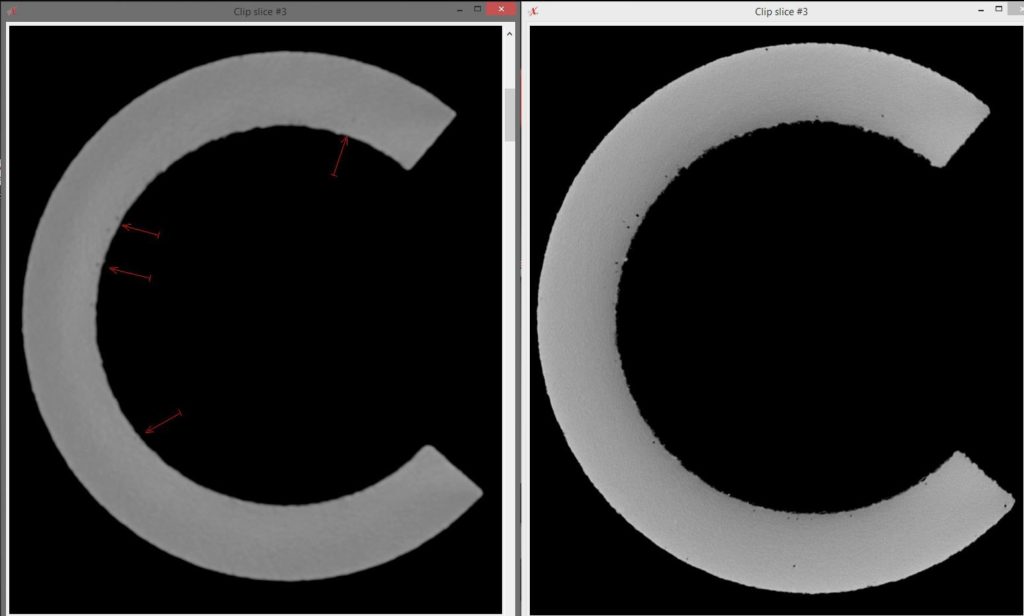
Let’s review the data from the Titanium additive sample. Two scans were performed in order to review and compare data about indication detection. Scan one was performed of the full sample and this yielded 45 micron scan data. This data was reconstructed and viewed for different types of indications. Indications of voiding or less dense inclusions and high density inclusions were present. From this data an isolated area was chosen for scan two. Scan two of this specific area, achieved a scan resolution of 15 micron. This 15 micron scan, with higher magnification now yields a smaller region of interest, image detail will be improved along with higher probability of detection. The figure of 45um data shows less dense indications appearing near the inner edge, they are visible, but appear blurry with low contrast. Viewing the 15um data image, with increased voxel data, the same indication now appear more sharp and well defined, increased contrast and definition is apparent.
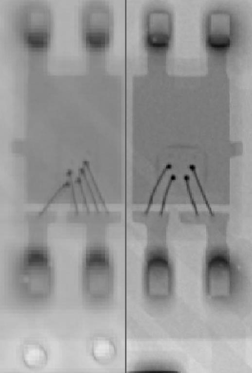
Computed Tomography additionally has the ability to take measurements internally and externally through your component. When viewing specific features on your component, wall thickness, feature to feature, the improved image quality from higher resolution scans will also make measurements more accurate. To further enhance measurement capability, a polygonal wire mesh can be applied to the surface, defining edges and features to allow for increased measurements accuracy. The data is stored in different point cloud data formats, .PLY, .STL, etc. This is then used for measurements or CAD comparison.
To conclude about using Computed Tomography on Aerospace additive manufactured components, the use is very obvious. We have a tool that can be used for defect detection, high to low density anomalies. This tool can be used to take measurements where conventional tools may not, especially the internals. Comparison of CAD data, from our known model to our production parts being made, we create the surface data using the wire mesh and create point cloud data for comparison. I hope this information was helpful in your journey with Additive Manufacturing.
Images